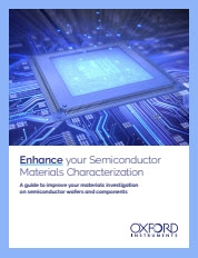
Enhance Your Semiconductor Materials Characterization
A Practical Guide for Improving Wafer and Component Analysis
The semiconductor industry is advancing at breakneck speed—pushing for faster, smaller, and more powerful devices. From 5G and AI to electric vehicles and advanced medical technologies, success depends on the precision of your materials characterization.As transistor and interconnect dimensions shrink below 10 nm, the margin for error is razor-thin. Defects, inconsistencies, and stress fields can severely impact device reliability and performance. This eBook illustrates how modern characterization tools enable:
Faster failure analysis and reverse engineering
Improved yield through earlier defect detection
Better material selection and process optimization
Streamlined quality assurance workflows
Download this free eBook and explore how cutting-edge analytical techniques—like SEM-EDS, BEX imaging, Raman spectroscopy, and atomic force microscopy—can help you stay ahead of the curve. Whether you're in R&D, process development, or manufacturing, this guide shows how to turn complex analytical data into actionable insights.
DOWNLOAD THIS EBOOK TO LEARN MORE
Become a member and enjoy exclusive benefits
Create an account now for exclusive benefits, personalized recommendations, and seamless order tracking. Elevate your lab experience today!