High-Resolution SEM-EDS Redefines Materials Analysis

Written By: LabX.com
May 16, 2025
Ultra-high-resolution SEM-EDS for advanced research and quality control
TESCAN introduces the MIRA XR, an ultra-high-resolution scanning electron microscope (SEM) integrated with energy-dispersive X-ray spectroscopy (EDS), designed for rapid and precise materials analysis in both academic and industrial settings. Bridging the gap between conventional field emission SEMs and ultra-high-resolution systems, the MIRA XR offers analytical flexibility, user-friendly operation, and streamlined workflows.
Key Features of the TESCAN MIRA XR
-
BrightBeam™ Technology: Achieves sub-nanometer resolution at low accelerating voltages, enabling detailed imaging of nanoscale structures.
-
Dual Essence™ EDS: Reduces elemental analysis turnaround time by up to 50%, enhancing workflow efficiency.
-
Wide Field Optics™: Speeds up sample navigation by 40%, facilitating quicker identification of regions of interest.
-
MultiVac™ Mode: Allows low-vacuum operation for beam-sensitive and outgassing samples, minimizing the need for extensive sample preparation.
-
In-Flight™ Automation: Simplifies imaging processes, making high-resolution imaging accessible to users of all experience levels.
The MIRA XR is engineered for high-throughput environments, including quality control, metallurgy, battery research, and semiconductor failure analysis, where both speed and imaging accuracy are critical.
Jan 09, 2026
Product News
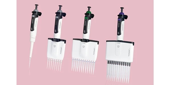
BRANDTECH Scientific Introduces the Transferpette® pro Micropipette: A New Twist on Comfort and Control
The latest addition to its trusted line of precision liquid handling instruments, engineered for comfort, control, and repeatable accuracy.

Jan 06, 2026
Featured, Technical Insight
New Research Frontiers Unlocked by Next-Generation Flow Cytometry
Next-generation flow cytometry systems using acoustic focusing are opening entirely new areas of research that were previously impractical or inaccessible with conventional flow cytometers.

Jan 05, 2026
Buying Guides
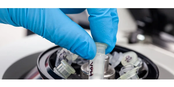
The Bottom Line: How Smart Microcentrifuge Tube Choices Impact Lab Efficiency and Cost
Innovative microcentrifuge tube solutions are more than just lab consumables—they’re strategic tools that can reduce costs, improve outcomes, and support long-term sustainability goals.

Jan 05, 2026
Buying Guides
Future-Proofing Your Lab with Innovative Microcentrifuge Tube Solutions
As laboratories evolve to meet the growing demands of modern science, even the most basic tools—like microcentrifuge tubes—are being reimagined.

Jan 05, 2026
Buying Guides
Microcentrifuge Tube Innovations: Driving Sustainable Change
Integrating next-generation consumables into standard workflows can lead to a more sustainable and responsible research environment.

Jan 05, 2026
Buying Guides
Single Use Plastics: How to Manage these Major Contributors to Lab Waste
Reducing lab waste isn’t just a sustainability issue—it’s a financial and operational one, too.
Jan 05, 2026
Buying Guides
Common Microcentrifuge Tube Challenges in Sensitive Molecular Workflows
Key factors that can impact the performance of microcentrifuge tubes for PCR, qPCR, and NGS and other sensitive applications

Jan 05, 2026
Buying Guides
How to Research the Right Microcentrifuge Tubes for Your Application
Selecting the right microcentrifuge tubes starts with understanding the specific demands of your application.

Jan 05, 2026
Technical Insight
The Best Confocal Microscopes of 2026
Discover the best confocal microscopes of 2026 for advanced imaging. Compare top models from Zeiss, Evident, and Nikon for speed, resolution, and budget.

Dec 24, 2025
Featured, Popular Products, Technical Insight
Emerging Mass Spectrometry Technologies to Improve Intraoperative Diagnostics
Advances in mass spectrometry may soon reshape surgery, improving diagnostic accuracy and impacting post-operative outcomes